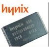
| 品牌:hyhns | 型号:HY27UF084G2B | 功率:30W |
Hynix NAND HY27UF(08/16)4G2B Series have 512Mx8bit with spare 16Mx8 bit capacity. The device is offered in 3.3 Vcc Power Supply, and with x8 and x16 I/O interface Its NAND cellrovides the most cost-effective solution for the solid state masstorage market. The memory is divided into blocks that can be erased independently so it is possible to preserve valid data while old data is erased.
The device contains 4096 blocks, composed by 64 pages.
A program operation allows to write the 2112-byte page in typical 200us and an erase operation can be performed in typical 1.5ms on a 128K-byte block.
Data in the page can be read out at 25ns cycle time per byt (x8). The I/O pins serve as the ports for address and data input/output as well as command input.
This interface allows a reduced pin count and easy migration towards different densities, without any rearrangement of footprint. Commands, Data and Addresses are synchronously introduced using CE, WE, RE ALE and CLE input pin. The on-chip Program/Erase Controller automates all read, program and erase functions including pulse repetition, where required, and internal verification and margining of data. The modify operations can be locked using the WP input. The output pin R/B (open drain buffer) signals the status of the device during each operation. In a system with multiple memories the R/B pins can be connected all together to provide a global status signal.
The copy back function allows the optimization of defective locks management. when a page program operation fails the data can be directly programmed in another page inside the same array section without the time consuming serial data insertion phase. Copy back operation automatically executes embedded error detection operation: 1 bit error every 528byte (x8) or 1bit error out of every 264-word (x16) can be detected. Due to this feature, it is no more nor necessary nor recommended to use external 2-bit ECC to detect copy back operation errors. Data read out after copy back read (both for single and multiplane cases) is allowed.
Even the write-intensive systems can take advantage of the HY27UF(08/16)4G2B Series extended reliability of 100K program/erase cycles by supporting ECC (Error Correcting Code) with real time mapping-out algorithm. The chip supports CE
don锟斤拷t care function. This function allows the direct download of the code from the NAND Flash memory device by a microcontroller, since the CE transitions do not stop the read operation.
This device includes also extra features like OTP/Unique ID area, Read ID2 extension.
The HY27UF(08/16)4G2B Series are available in 48-TSOP1 12 x 20 mm.