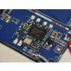
| Ʒ�ƣ�ESMT | �ͺţ�M15T1G1664A-DEBG2CS | ���ͣ��洢�� |
| �洢������1G | �������64*16 | ��װ��BGA |
| ���ţ�2018+ | Ӧ�������������ӡ� ����ͨ�š� ҽ�Ƶ��ӡ� ���ܼҾӡ� ���õ����� ������IoT |
Feature |
Interface and Power Supply
SSTL_135: VDD/VDDQ = 1.35V(-0.067V/+0.1V)
SSTL_15: VDD/VDDQ = 1.5V(±0.075V)
JEDEC DDR3(L) Compliant
8n Prefetch Architecture
Differential Clock (CK/ CK ) and Data Strobe (DQS/ DQS )
Double-data rate on DQs, DQS and DM
Data Integrity
Auto Refresh and Self Refresh Modes
Power Saving Mode
Partial Array Self Refresh(PASR) Power Down Mode
Signal Integrity
Configurable DS for system compatibility Configurable On-Die Termination
ZQ Calibration for DS/ODT impedance accuracy via external ZQ pad (240 ohm ± 1%)

Signal Synchronization
Write Leveling via MR settings Read Leveling via MPR
Programmable Functions
CAS Latency (5/6/7/8/9/10/11/12/13) CAS Write Latency (5/6/7/8/9)
Additive Latency (0/CL-1/CL-2)
Write Recovery Time (5/6/7/8/10/12/14/16) Burst Type (Sequential/Interleaved)
Burst Length (BL8/BC4/BC4 or 8 on the fly)
Self Refresh Temperature Range(Normal/Extended) Output Driver Impedance (34/40)
On-Die Termination of Rtt_Nom(20/30/40/60/120) On-Die Termination of Rtt_WR(60/120)
Precharge Power Down (slow/fast)
Ordering Information
Product ID | Max Freq. | VDD | Data Rate | Package | Comments | |
(CL-tRCD-tRP) | ||||||
M15T1G1664A–BDBG2C | 800MHz | 1.35V/1.5V | DDR3(L)-1600 (11-11-11) | 96 ball BGA | Pb-free | |
(7.5mmx13.5mm) | ||||||
M15T1G1664A–DEBG2C | 933MHz | 1.35V/1.5V | DDR3(L)-1866 (13-13-13) | Pb-free | ||
M15T1G1664A–BDBG2CS | 800MHz | 1.35V/1.5V | DDR3(L)-1600 (11-11-11) | 96 ball BGA | Pb-free | |
(7.5mmx13mm) | ||||||
M15T1G1664A–DEBG2CS | 933MHz | 1.35V/1.5V | DDR3(L)-1866 (13-13-13) | Pb-free | ||
������̩�ӵ�������˾ �ֻ���𐀍𐀎𐀏𐀐𐀐𐀎𐀑𐀒𐀍𐀑 �绰��𐀓𐀏𐀐𐀐𐀔𐀕𐀕𐀍𐀓𐀖𐀐𐀏 ��ַ���㶫 ���� ������ �������������Ƿ�ʹ���A-7A